|
Архитектура Аудит Военная наука Иностранные языки Медицина Металлургия Метрология Образование Политология Производство Психология Стандартизация Технологии |
|
|
Архитектура Аудит Военная наука Иностранные языки Медицина Металлургия Метрология Образование Политология Производство Психология Стандартизация Технологии |
Components of an Image Processing System
This section briefl y outlines the capabilities of modern image processing systems. A general purpose image acquisition and processing system typically consists of four essential components: 1. An image acquisition system. In the simplest case, this could be a CCDcamera, a fl atbed scanner, or a video recorder. 2. A device known as a frame grabber to convert the electrical signal (normally an analog video signal) of the image acquisition system into a digital image that can be stored. 3. A personal computer or a workstation that provides the processing power. 4. Image processing software that provides the tools to manipulate and analyze the images.
Image Sensors Digital processing requires images to be obtained in the form of electrical signals. These signals can be digitized into sequences of numbers which then can be processed by a computer. There are many ways to convert images into digital numbers. Here, we will focus on video technology, as it is the most common and aff ordable approach. The milestone in image sensing technology was the invention of semi- conductor photodetector arrays. There are many types of such sensors, the most common being the charge coupled device or CCD. Such a sensor consists of a large number of photosensitive elements. During the accu- mulation phase, each element collects electrical charges, which are gen- erated by absorbed photons. Thus the collected charge is proportional 22 1 Applications and Tools
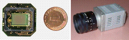
A b
Figure 1.17: Modern semiconductor cameras: a Complete CMOS camera on a chip with digital and analog output (image courtesy, K. Meier, Kirchhoff -Institute for Physics, University of Heidelberg), [114]). b High-end digital 12-bit CCD cam- era, Pixelfl y (image courtesy of PCO GmbH, Germany).
to the illumination. In the read-out phase, these charges are sequentially transported across the chip from sensor to sensor and fi nally converted to an electric voltage. For quite some time, CMOS image sensors have been available. But only recently have these devices attracted signifi cant attention because the image quality, especially the uniformity of the sensitivities of the individual sensor elements, now approaches the quality of CCD image sensors. CMOS imagers still do not reach up to the standards of CCD imagers in some features, especially at low illumination levels (higher dark current). They have, however, a number of signifi cant advantages over CCDimagers. They consume signifi cantly less power, subareas can be accessed quickly, and can be added to circuits for image preprocess- ing and signal conversion. Indeed, it is possible to put a whole camera on a single chip (Fig. 1.17a). Last but not least, CMOS sensors can be manufactured more cheaply and thus open new application areas. Generally, semiconductor imaging sensors are versatile and powerful devices:
1.7 Components of an Image Processing System 23
But if CCDdevices are cooled down to low temperatures, they can be exposed for hours. Such devices are commonly used in astronomy and are about one hundred times more sensitive than photographic material.
|
Последнее изменение этой страницы: 2019-05-04; Просмотров: 198; Нарушение авторского права страницы