
|
Архитектура Аудит Военная наука Иностранные языки Медицина Металлургия Метрология Образование Политология Производство Психология Стандартизация Технологии |
|
|
Архитектура Аудит Военная наука Иностранные языки Медицина Металлургия Метрология Образование Политология Производство Психология Стандартизация Технологии |
UNIT –I DEFECTS IN CRYSTALSСтр 1 из 8Следующая ⇒
UNIT –I DEFECTS IN CRYSTALS Structure Introduction 1.1 Objectives 1.2 Point Defect in ionic crystals and metals 1.3 Diffusion in solids 1.3.1 Type of Diffusion 1.3.2 Diffusion Mechanisms 1.3.3 Diffusion Coefficient 1.3.4 Applications 1.4 Ionic Conductivity 1.5 Colour Centres 1.5.1 F- Centres 1.5.2 V-Centres 1.6 Excitions 1.7 General Idea of Luminescence 1.8 Dislocations & Mechanical Strength of Crystals 1.9 Plastic Bahaviour 1.10 Type of Dislocations 1.11 Stress field of Dislocations 1.12 Grain Boundaries 1.13 Etching- Types of Etching 1.14 Let Us Sum Up 1.15 Check Your Progress: The Key
INTRODUCTION
Up to now, we have described perfectly regular crystal structures, called ideal crystals and obtained by combining a basis with an infinite ·space lattice. In ideal crystals atoms were arranged in' a regular way. However, the structure of real crystals differs from that of ideal ones. Real crystals always have certain defects or imperfections, and therefore, the arrangement of atoms in the volume of a crystal is far from being perfectly regular. Natural crystals always contain defects, often in abundance, due to the uncontrolled conditions under which they were formed. The presence of defects which affect the colour can make these crystals valuable as gems, as in ruby (chromium replacing a small fraction of the aluminium in aluminium oxide: Al203). Crystal prepared in laboratory will also always contain defects, although considerable control may be exercised over their type, concentration, and distribution.
Key a = vacancy (Schottky defect) b = interstitial c = vacancy – interstitial pair (Frenkel defect) d = divacancy e = split interstitial
The Main aim of this unit is to study defect in crystals after going through the unit you should be able to · Describe the type of defects · Explain the diffusion in crystal · Explain the color center and excitations · Explain the type of dislocation Check Your Progress 2 Notes : (i) Write your answer in the space given below (ii) Compare your answer with those given at the end of the unit What are crystal defects and how are they classified? …………………………………………………………………………………… …………………………………………………………………………………… …………………………………………………………………………………… …………………………………………………………………………………… DIFFUSION
Diffusion refers to the transport of atoms through a crystalline or glassy solid. Many processes occurring in metals and alloys, especially at elevated temperatures, are associated with self-diffusion or diffusion. Diffusion processes play a crucial 'role in many solid-state phenomena and in the kinetics of micro structural changes during metallurgical processing and applications; typical examples include phase transformations, nucleation, recrystallization, oxidation, creep, sintering, ionic conductivity, and intermixing in thin film devices. Direct technological uses of diffusion include solid electrolytes for advanced battery and fuel cell applications, semiconductor chip and microcircuit fabrication and surface hardening of steels through carburization. The knowledge of diffusion phenomenon is essential for the introduction of a very small concentration of an impurity in a solid state device: Types of Diffusion (i) Self Diffusion: It is the transition of a thermally excited atom from a site of crystal lattice to an adjacent site or interstice. (ii) Inter Diffusion: This is observed in binary metal alloys such as the Cu-Ni system. iii) Volume Diffusion: This type of diffusion is caused due to atomic movement in bulk in materials. (iv) Grain Boundary Diffusion: This type of diffusion is caused due to atomic movement along the grain boundaries alone.
along the surface of a phase. Diffusion Mechanisms
Diffusion is the transfer of unlike atoms which is accompanied with a change of concentration of the components in certain zones of an alloy. Various mechanisms have been proposed to explain the processes of diffusion. Almost all of these mechanisms are based on the vibrational energy of atoms in a solid. Direct-interchange, cyclic, interstitial, vacancy etc. are the common diffusion mechanisms. Actually, however, the most probable mechanism of diffusion is that in which the magnitude of energy barrier (activation energy) to be overcome by moving atoms is the lowest. Activation energy depends on the forces of interatomic bonds and crystal lattice defects, which facilitate diffusion transfer (the activation energy at grain boundaries is only one half of that in the bulk of a grain). For metal atoms, the vacancy mechanism of diffusion is the most probable and for elements with a small atomic radius (H, N and C), the interstitial mechanism. Now, we will study these mechanisms. (i) Vacancy Mechanism: This mechanism is a very dominant process for diffusion in FCC, BCC and HCP metals and solid solution alloy. The activation energy for this process comprises the energy required to create a vacancy and that required to move it. In a pure solid, the diffusion by this mechanism is shown in Fig. 3(a). Diffusion by the vacancy mechanism can occur by atoms moving into adjacent sites that are vacant. In a pure solid, during diffusion by this mechanism, the atoms surrounding the vacant site shift their equilibrium positions to adjust for the change in binding that accompanies the removal of a metal ion and its valency electron. We can assume that the vacancies move through the lattice and produce random shifts of atoms from one lattice position to another as a result of atom jumping. Concentration changes takes place due to diffusion over a period of time. We must note that vacancies are continually being created and destroyed at the surface, grain boundaries and suitable interior positions, e.g. dislocations. Obviously, the rate of diffusion increases rapidly with increasing temperature.
If a solid is composed of a single element, i.e. pure metal, the movement of thermally excited atom from a site of the crystal lattice to an adjacent site or interstice is called self diffusion because the moving atom and the solid are the same chemical-element. The self-diffusion in metals in which atoms of the metal itself migrate in a random fashion throughout the lattice occurs mainly through this mechanism. We know that copper and nickel are mutually soluble in all proportions' in solid state and form substitutional solid solutions, e.g., plating of nickel on copper. For atomic diffusion, the vacancy mechanism is shown in Fig. 4.
changes positions using an interstitial site does not usually occur in metals for elf-diffusion but is favored when interstitial impurities are present because of the low activation energy. When a solid is composed of two or more elements whose atomic radii differ significantly, interstitial solutions may occur. The large size atoms occupy lattice sites where as the smaller size atoms fit into the voids (called as interstices) created by the large atoms. We can see that the diffusion mechanism in this case is similar to vacancy diffusion except that the interstitial atoms stay on interstitial sites (Fig. 3(b)). We must note that activation energy is associated with interstitial diffusion because, to arrive at the vacant site, it must squeeze past neighbouring atoms with energy supplied by the vibrational energy of the moving atoms. Obviously, interstitial diffusion is a thermally activated process. The interstitial mechanism process is simpler since the presence of vacancies is not required for the solute atom to move. This mechanism is vital for the following cases: (a) The presence of very small atoms in the interstices of the lattice affect to a great extent the mechanical properties of metals. (b) At low temperatures, oxygen, hydrogen and nitrogen can be diffused in metals easily. (iii) Interchange Mechanism: In this type of mechanism, the atoms exchange places through rotation about a mid point. The activation energy for the process is very high and hence this mechanism is highly unlikely in most systems. Two or more adjacent atoms jump past each other and exchange positions, but the number of sites remains constant (Fig. 3 (c) and (d)). This interchange may be two-atom or four-atom (Zenner ring) for BCC. Due to the displacement of atoms surrounding the jumping pairs, interchange mechanism results in severe local distortion. For jumping of atoms in this case, much more energy is required. In this mechanism, a number of diffusion couples of different compositions' are produced, which are objectionable. This is also termed as Kirkendall's effect.
From theoretical point of view, Kirkendall's effect is very important in diffusion. We may note that the practical importance of this effect is in metal cladding, sintering and deformation of metals (creep). 1.3.3 Diffusion Coefficient: Fick’s Laws of Diffusion Diffusion can be treated as the mass flow process by which atoms (or molecules) change their positions relative to their neighbours in a given phase under the influence of thermal energy and a gradient. The gradient can be a concentration gradient; an electric or magnetic field gradient or a stress gradient. We shall consider mass flow under concentration gradients only. We know that thermal energy is necessary for mass flow, as the atoms have to jump from site to site during diffusion. The thermal energy is in the form of the vibrations of atoms about their mean positions in the solid. The classical laws of diffusion are Fick's laws which hold true for weak solutions and systems with a low concentration gradient of the diffusing substance, dc/dx (= C2 – C1/X2 – X1), slope of concentration gradient. (i) Fick's First Law: This law describes the rate at which diffusion occurs. This law states that
i.e. the quantity dn of a substance diffusing at constant temperature per unit time t through unit surface area a is proportional to the concentration gradient dc/dx and the coefficient of diffusion (or diffusivity) D (m2/s). The 'minus' sign implies that diffusion occurs in the reverse direction to concentration gradient vector, i.e. from the zone with a higher concentration to that with a lower concentration of the diffusing element. The equation (2) becomes:
 (3) (3)
where J is the flux or the number of atoms moving from unit area of one plane to unit area of another per unit time, i.e. flux J is flow per unit cross sectional area per unit time. Obviously, J is proportional to the concentration gradient. The negative sign implies that flow occurs down the concentration gradient. Variation of concentration with x is shown in Fig. 5. We can see that a large negative slope corresponds to a high diffusion rate. In accordance with Fick's law (first), the B atoms will diffuse from the left side. We further note that the net migration of B atoms to the right side means that the concentration will decrease on the left side of the solid and increase on the right as diffusion progress.
This law can be used to describe flow under steady state conditions. We find that it is identical in form to Fourier's law for heat flow under a constant temperature gradient and Ohm's law for current flow under a constant electric field gradient. We may see that under steady state flow, the flux is independent of time and remains the same at any cross-sectional plane along the diffusion direction.
Parentheses indicate that the phase is metastable (ii) Fick’s second Law: This is an extension of Fick’s first law to non steady flow. Frick’s first law allows the calculation of the instaneous mass flow rate (Flux) past any plane in a solid but provides no information about the time dependence of the concentration. However, commonly available situations with engineering materials are non-steady. The concentration of solute atom changes at any point with respect to time in non-steady diffusion. If the concentration gradient various in time and the diffusion coefficient is taken to be independent of concentration. The diffusion process is described by Frick’s second law which can be derived from the first law: Equation 4 Fick’s second law for unidirectional flow under non steady conditions. A solution of Eq. (4)given by Where A is constant Let us consider the example or self diffusion or radioactive nickel atoms in a non-radioactive nickel specimen. Equation (4a) indicates that the concentration at x = 0 falls with time as r-12 and as time increases the radioactive penetrate deeper in the metal block [Fig.6 ] At time t1 the concentration of radioactive atoms at x = 0 is c1= A/(Dt1)1/2. At a distance x1 = 0 (Dt1)1/2 the concentration falls to 1/e of c1. At time t2 . the concentration at x = 0 is c2 = A/(Dt2)1/2 and this falls to 1/e and x2 = 2 (Dt2)1/2 . These results are in agreement with experiments.
If D is independent of concentration, Eq. (4) simplifies to
Even though D may vary with concentration, solutions to the differential Eq. 5 are quite commonly used for practical problems, because of their relative simplicity. The solution to Eq.5 for unidirectional diffusion from one medium to another a cross a common interface is of the general form. Where A and B are constant to be determined from the initial and boundary conditions of a particular problem. The two media are taken to be semi-infinite i.e. only one end of each of them, which the interface is defined. The other two ends are at an infinite distance The initial uniform concentrations of the diffusing species in the two media are different, with an abrupt change in concentrations at the interface erf in eqn.5 (a) stands for error function, which is his an integration variable, that gets deleted as the limits of the integral are substituted. The lower limits of the integral is always zero, while the upper limit of the integral is the quantity, whose function is to be determined
A schematic illustration of time dependence of diffusion is shown in fig7. The curve corresponding to the concentration profile at a given instant of time t1 is marked by t1. We can see from fig.7 at a later time t2, the concentration profile has changed. We can easily see that this changed in concentration profile is due to the diffusion of B atoms that has occurred in the time interval t2-t1 The concentration profile at a still later time t3 is marked by t3 . Due to diffusion, B atoms are trying to get distributed uniformaly throughout the solid salutation. From Fig. 7 Its is evident that the concentration gradient becoming less negative as time increases. Obviously, the diffusion rate becomes slower as the diffusion process progress.
Factors Affecting Diffusion Coefficient (D) We have mentioned that diffusion co-efficient is affected by concentration. However, this effect is small compared to the effect of temperature. While discussion diffusion mechanism, we have assumed that atom jumped from one lattice position to another. The rate at which atoms jumped mainly depends on their vibrational frequency, the crystal structure. Activation energy and temperature we may note that at the position. To overcome this energy barrier, The energy required by the atom is called the activation of diffusion (Fig. 8)
Fig. 8. Activation energy for diffusion (a) vacancy mechanism (b) interstitial mechanism The energy is required to pull the atom away from its nearest atoms in the vacancy mechanism energy is also required top force the atom into closer contact with neighbouring atoms as it moves along them in interstitial diffusion. If the normal inter- atomic distance is either increases or decrease, addition energy is required. We may note that the activation energy depends on the size of the atom. i.e. it varies with the size of the atom, strength of bond and the type of the diffusion mechanism. It is reported that the activation energy required is high for large- sized atoms, strongly bonded material , e.g. corundum and tungsten carbide (since interstitial diffusion requires more energy than the vacancy mechanism.)
Diffusion processes are the basis of crystallization recrystallization, phase transformation and saturation of the surface of alloys by other elements, Few important applications of diffusion are : (i) Oxidation of metals (ii) Doping of semiconductors. (iii) Joining of materials by diffusion bonding, e.g. welding, soldering, galvanizing, brazing and metal cladding (iv) Production of strong bodies by sintering i.e. powder metallurgy. (v) Surface treatment , e.g. homogenizing treatment of castings , recovery, recrystallization and precipitation of phases. (vi) Diffusion is fundamental to phase changed e.g. y to a-iron.
Fig. 9. C gradient in 1022 steel carburized in 1.6% CH4, 20% CO and 4%H.
Check Your Progress 3 Notes : (i) Write your answer in the space given below (ii) Compare your answer with those given at the end of the unit What is diffusion and on what variable it depends? ……………………………………………………………………………………… ……………………………………………………………………………………… ……………………………………………………………………………………… ………...……………………………………………………………………………
IONIC CONDUCTIVITY
It is known that the dominant lattice defect responsible for the ionic conductivity in pure and doped lead chloride is the anion vacancy (Jost 1952). The activation energy for migration of the anion vacancy has been measured by Simkovich (1963), Seith (De Vries 1965) and Gylai (De Vries 1965) in powder samples and is found to range from 0-48 eV to 0-24 eV. The measurements on single crystals of pure and doped lead chloride, however, show that the energy of formation of vacancies is 1-66 eV and that for migration of the anion vacancies is 0-35 eV (De Vries and Van Santen 1963; De Vries 1965). Theroles of various point defects in this material are not yet clearly understood. Simkovich, fox example, concluded that in the extrinsic region half of the anion vacancies are associated with cation vacancies to form charged pairs. Barsis and Taylor (1966), on the other hand, proposed that appreciable number of inteistitials, i.e., unassociated Frenkel defects, are present in the extrinsic region as seen from the analysis of isotherms obtained by them from the data of De Vries and Van Santen. The recent experiments by Van den Brom etal (1972) on the dielectric relaxation in pure lead chloride suggest that in this region dipole species such as anion vacancy-impurity associates are piesent. In this paper, we shall present the results of self-diffusion and ionic conductivity measurements made on pure crystals of lead chloride, and show that ir this material Schottky defects are mainly responsible for the observed ionic transport and that the impurity anion vacancy associates, particularly the oxygen ions, influence it markedly in the extrinsic region.
1.5 COLOUR CENTRES Colour centres: Becquerel discovered that a transparent NaCl crystal was coloured yellowish when it was placed near a discharge tube. The colouration of the NaCl and other crystals was responsible for the study of colour centres. Actually, rocksalt should have an infrared absorption due to vibrations of its ions and an ultraviolet absorption due to the excitation of the electrons. A perfect NaCl crystal should not absorb visible light and so it should be perfectly transparent. This leads us to the conclusion that the colouration of crystals is due to defects in the crystals. It is also found that exposure of a coloured crystal to white light can result in bleaching of the colour. This gives further clues to the nature of absorption by crystals. Experiments show that during the bleaching of the crystal the crystal becomes photoconductive. i.e., electrons are excited to the conduction band. Photoconductivity tells us about the quantum efficiency (number of free electrons produced per incident photon) of the colour centres. It is known that insulators have large energy gaps and that they are transparent to visible light. Ionic crystals have the forbidden energy gap of about 6eV which corresponds to a wavelength of about 2000A0 in the ultraviolet region. From dielectric properties we know that the ionic polarizability resonates at a wavelength of 60 microns in the far infrared region. It is why these crystals are expected to be transparent over a wide range of spectrum including the visible region. Due to such a good transparency, the crystals of KCl, NaCl, LiF and other alkali halides are used for making prisms, lenses and optical windows in optical and infrared spectrometers. However, due to different reasons, absorption bands may occur in the visible, near ultraviolet and near infrared regions in these crystals. If the absorption band is in the visible region and the band is quite narrow, it gives a characteristic colour to the crystal. When the crystal gets coloured, it is said to have colour centres. Thus a colour centre is a lattice defect, which absorbs light.
(i) Crystals can be coloured by the addition of suitable chemical impurities like transition element ions with excited energy levels. Hence alkali halide crystals can be coloured by ions whose salts are normally coloured. (ii) The crystals can be coloured by introducing stoichiometric excess of the cation by heating the crystal in the alkali metal vapour and then cooling it quickly. The colours produced depend upon the nature of the crystals e.g., LiF heated in Li vapour colours it pink, excess of K in KCl colours it blue and an excess of Na in NaCl makes the crystal yellow. Crystals coloured by this method on chemical analysis show an excess of alkali metal atoms, typically 1016 to 1019 per unit volume. (iii) Crystals can also be coloured or made darker by exposing them to high energy radiations like X-rays or ϒ-rays or by bombarding them with energetic electrons or neutrons.
4650A 0 and it is called the F band. This absorption in the blue region is said to be responsible for the yellow colour produced in the crystal. The F band is characteristic of the crystal and not of the alkali metal used in the vapour i.e., the F band in KCI or NaCl will be the same whether the crystal is heated in a vapour of sodium or of potassium. The F bands associated with the F centres of some alkali halide crystals are shown in fig. 10, in which the optical absorption has been plotted against wavelength or energy in eV
Formation of F-Centres: Colour centres in crystals can be fanned by their non-stoichiometric properties i.e., when crystals have an excess of one of its constituents. NaCl crystal can therefore be coloured by heating it in an atmosphere of sodium vapour and then cooling it quickly. The excess sodium atoms absorbed from the vapour
Split up into electrons and positive ions in the crystal (fig. 11). The crystal becomes slightly non-stoichiometric, with more sodium ions than chlorine ions. This results in effect in CI- vacancies. The valence electron of the alkali atom is not bound to the atom, it diffuses into the crystal and becomes bound to a vacant negative ion site at F because a negative ion vacancy in a perfect periodic lattice has the effect of an isolated positive charge. It just traps an electron in order to maintain local charge neutrality. The excess electron captured in this way at a negative ion vacancy in an alkali halide crystal is called an F centre. This electron is shared largely by the six positive metal ions adjacent to the vacant negative lattice site as shown in 2-dimensions by the dotted circle in fig. 11. The figure shows an anion vacancy and an anion vacancy with an associated electron, i.e., the centre. This model was first suggested by De-Boer and was further developed by Mott and Gurney. Change of Density: Since some Cl- vacancies are always present in a NaCl crystal in thermodynamic equilibrium, any sort of radiation which will cause electrons to be knocked into the Cl- vacancies will cause the formation of F centres. This explains Becquerel's early results also. With that the generation of vacancies by the introduction of excess metal can be experimentally demonstrated by noting a decrease in the density of the crystal. The change of density is determined by X-ray diffraction measurements.
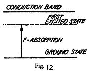
shows the energy level diagram for an F centre. It also shows that the F absorption band is produced due to a transition from the ground state to the first excited state below the conduction band. Effect of temperature on F-band: We have seen above that the energy levels of an F-centre depend upon the atomic surroundings of vacancy. This means that the absorption peak should shift to shorter wavelengths i.e., higher energies when the interatomic distances in the crystal are decreased. This shift is actually observed on varying the temperature of the crystal. The absorption maximum has a finite breadth even at very low temperature, which increases on increasing the temperature of the crystal. It can be explained by studying the dependence of the energy of-a colour centre on temperature. Fig. 13. Shows a graph plotted between the changes in energy of an electron in F centre and the coordination of a vacancy
state of that electron.
At any finite temperature the ground state is not at 0, the minimum of curve G but lies above it by about kE because the coordinating ions vibrate between A and B due to thermal energy. Hence the energy of the absorbed radiation can range between that of transition A → A` or B → B`. The difference between energies, corresponding to A` and B` gives the width of the absorption peak. AB represents the amplitude of vibration of ions at a lower temperature but as the temperature rises it moves to a higher energy position so that CD represents the amplitude of vibration at the higher temperature and thus the width of the absorption peak- the F band increases. Klcinschord observed that the F band instead of being exactly like a bell, ossesses a shoulder and a tail on the short wavelength side. Seitz called the shoulder as a K-band and it may be considered to be due to transitions of the electron to excited states, which lie between the first excited state and the conduction band. The tail may be supposed to be due to the transition from the ground state of F-centre to the conduction band. Magnetic Properties of F-Centres: In fig. 13, the upper curve E is determined by the change in the surroundings of a vacancy when the trapped electrons is in the excited state. This is usually expressed by a change of the effective dielectric constant in the neighbourhood of such a vacancy. An alkali halide crystal is normally diamagnetic because the ions have closed outer shells. Since an F-centre contains an unpaired trapped electron, crystals additively coloured with a metal have some paramagnetic behavior. Thus the structure of F-centres can be studied by electron paramagnetic resonance experiments which tell us about the wave-functions of the trapped electron.
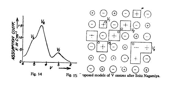
maxima which are called as V1, V2 bands and so on. Mollwo was able to introduce access halogen into KBr and KI and found that it is was not possible in case of KCl. He shows that by heating KI in iodine vapour ,new absorption bands are obtain in the ultraviolet .the bands obtain by Mollwo for KBr when heated in Br2 vapour are shown in fig. 14, having V1, V 2 and V3 bands.
It can be understood that the strong peak observed by Mollwo in KBr as shown in fig. 14 is however, not of the above type. Mollwo's experiment proves that the saturation density of colour centres is proportional to the number of bromine molecules at a particular temperature. By the law of mass action, we know that one colour centre should be produced by each molecule absorbed from the vapour. Hence it was proposed by F. Seitz that the centres associated with the strong peak are of molecular nature, i.e., two holes are trapped by two positive ion vacancies. Such a centre is called a V2 centre and is shown in fig. 15. As is evident from the figures 13 and 15, the V1 centre is the counterpart of the F-centre, V2 and V3 are those of the R centres and V 4 is the counterpart of the M centre. However, the identification of the V1 centre with the V 1 band is uncertain because the spin resonance results of Kaenzig suggest that a centre having the symmetry of the V3 centre produces the V1 band. The detailed properties of V centres have not yet been properly understood. Production or Colour Centres by X-rays or Particle Irradiation: The colour centres can also be produced in crystals by irradiating them with very high energy radiation like X -rays or ϒ rays. An X-ray quantum when passes through an ionic crystal produces fast photo electrons having the energy nearly equal to that of the incident quantum. These high energy electrons interact with the valence electrons in the crystal and lose their energy by producing free electrons and holes, excitons (electron hole pairs) and phonons. These free electrons and holes diffuse into the crystal and come across vacancies present in the crystal where they may be caught producing trapped electrons and holes. In this way both F and V types of colour centres are produced in crystals irradiated with high energy radiations. However, these are not permanent like those produced in non stoichiometric crystals in which there is an internally produced excess of electrons and holes. Their colours cannot be removed permanently without changing them chemically. The colour centres produced by X-ray radiation are easily bleached by visible light or by heating because the excited electrons and holes ultimately recombine with each

other. The F and V centres produced by irradiation with 30 keV X -rays at room temperature (20°C) have been shown in fig. 16 in the absorption spectrum of KCl taken by Dorendorf and Pick. Check Your Progress 4 Notes : (i) Write your answer in the space given below (ii) Compare your answer with those given at the end of the unit What are color centers and how do they affect electric conductivity of solids? ……………………………………………………………………………………… ……………………………………………………………………………………… ……………………………………………………………………………………… ………...……………………………………………………………………………
EXCITIONS The most obvious point defects consist of missing ions (vacancies), excess ions (interstitials), or the wrong kind of ions (substitution impurities). A more subtle possibilitials is the case of an ion in a perfect crystal, that differs from its colleagues only by being in an excited electronic state. Such a “defect” is called a Frenkel exciton. Since any ion is capable of being so excited, and since the coupling between the ions’ outer electronic shells is strong, the excitation energy can actually be transferred from ion to ion . Thus the Frenkel exciton can move through the crystal wit\hout the ions themselves having to change places, as a result of which it is (like the polaron) for more mobile than vacancies, interstitials, or substitutional impurities. Indeed, for more accurate to describe the electronics structure of a crystal containing an exciton, as a quantum mechanical superposition of states, in which it is equally probable that the excitation is associated with any ion in the crystal. This latter view bears the same relation to specific excited ions, as the Bloch tight – binding levels (Chapter 10) bear to the individual atomic levels, in the theory of band structures.
Suppose we have calculated the electronic ground state of an insulator in the independent electron approximation. The lowest excited state of the insulator willevidently be given by removing one electron from the highest level in the highest occupied band 9the valence band) and placing it into the lowest – lying level of the lowest unoccupied band (conduction band). Such a rearrangement of the distribution of electrons does not alter the self- consistent periodic potential in which they move. This is because the Bloch electron are not localized (since | ynk(r)|2 is periodic), and therefore the change in local charge density produced by changing the level of a single electron will be of order 1/N (since only an Nth of the electron's charge will be in any given cell) i.e. negligibly small. Thus the electronic energy levels do not have to be recomputed for the excited configuration and the first excited state will lie an energy ec -ev above the energy of the ground state, where ec is the conduction band minimum and ev the valence band maximum. However, there is another way to make an excited state. Suppose we form a one-electron level by superposing enough level near the conduction band minimum to form a well- localized wave packet. Because we need levels in the neighborhood of the minimum to produce the wave packet, the energy ec of the wave packet will be somewhat grater than ec. Suppose in addition that the valence band level we depopulate is also wave packet. , formed of levels in the neighborhood of the valence band maximum (so that its energy ev is somewhat less than ev) and chosen so that the center of the wave packet is spatially very near the center of the conduction band wave packet. If we ignored electron – electron interactions, the energy required to move an electron from valence to conduction band wave packet. If we ignored electron- electron interactions, the energy required to move an electron from valence to conduction band wave packets would be ec - ev > ec - ev, but because the levels are localized, there will, in addition, be a non – negligible amount of negative Coulomb energy due to the electrostatic attraction of the (localized) conduction band electron and (localized) valence band hole.
Let us consider the case in which the localized electron and hole levels extend over many lattice constants. We may then make the same type of semi classical argument that we used to deduce the form of the impurity levels in semiconductors. We regard the electron and hole as particles of mass mc and mv (the conduction and valence band effective masses, which we take, for simplicity, to be isotropic). They interact through an attractive Coulomb interaction screened by the dielectric constant Î of the crystal. Evidently this is just the hydrogen atom problem, with the hydrogen atom reduced mass m (1/m = 1/Mproton + 1/melectron » 1/melectron) replaced by the reduced effective mass m* (1/m* = 1/mc + 1/mv ) , and the electronic charge replaced by e2/Î. Thus there will be bound states, the lowest of which extends over a Bohr radius given by:.

the energy of the bound state will be lower than the energy (ec - ev ) of the non-interacting electron and hole by
The validity of this model requires that aex be large on the scale of the lattic (i.e., aex >>a0), but since insulators with small energy gaps tend to have small effective masses and large dielectric constants, that is no difficult to achieve, particularly in semiconductors. such hydrogenic spectra have in fact been observed in the optical absorption that occurs below the inter and threshold. The exciton described by this model is known as the Mott- Wannier exciton Evidently as the atomic levels out of which the band levels are formed become more tightly bound Îwill decrease m* will increases, a0* will decrease, the exciton will become more localized, and the Mott- Wannier picture will eventually break down. The Mott- Wannier exciton and the Frenkel exciton are opposite extremes of the same phenomenon. In the Frenkel case, based as it is on a single excited ionic level, the elelctron and hole are sharply localized on the atomic scale. The exciton spectra of the solid range gases fall in this class. Fig. 19
shear stress t has been plotted as a function of the relative displacement of the planes from their equilibrium positions and this gives the periodic behavior of t as supposed by Frenkel. ' t is found to become zero for x = 0, a/2, a etc., where a is the distance between the atoms in the direction of the shear. Frenkel assumed that this periodic function is given by where the amplitude In order to calculate the force required to shear the two planes of atoms, we from the definition of shear modulus
where G is the shear module and
or This gives the maximum critical stress above which the crystal becomes unstable. It is about one sixth of the shear modulus. In a cubic crystal, G c44 = 1011 dynes per cm. for a shear in the <100> direction. Hence the theoretical value of the critical shear stress on Frenkel's model is tc = 1010 dynes per sq. .cm. which is much larger than the observed values for pure crystals. However., the experimental values for the maximum resolved shear stress required to start the plastic flow in metals were of the order of 10-3 to 10-4 G at that time and it was not a agreement with the results of eqn.. (10) Later it was considered that eqn (10) gave a higher value as the different semi-inter –atomic force of Fig.19 (b) as taken by Frenkel. The above disagreement may also be due to other special configuration of mechanical stability which the lattice may develop when it is sheared. Mackenzie in 1949, using central forces in the case of close packed lattices found that tc could be reduced to a value G/30 , corresponding to a critical shear strain of about 20 This value, however, is supposed to be an underestimate due to the neglect of the small directional force which are also present in such lattices. The contributions of thermal stresses also reduce tc below G/30 only near the melting point. Thus at room temperature we should have G/5 > tc > G/30 i.e. = G/15. In the case of whiskers only,. the experimental value of tc for various metals has been found to be of this order which is in excellent agreement with the theoretical result. Recent experimental work on bulk copper and zinc has shown that plastic deformation being at stresses of the order of 10-9 G. Hence, except for whiskers the disagreement is even larger than before.. It is therefore clear that agreement between theory and experiment be obtained on the basis of Frenkel's model where atomic plant glide past each other assuming fig. 19 (a) that the atoms of the upper atomic plane move simulantaneously relative to the lower plane. This assumption is based on the supposition of a perfect lattices, and that is the main cause of difficulty. We have , therefore, to consider the presence of imperfections which act as sources of mechanical weakness in actual crystals and which may proud a slip by the consecutive motion of the atoms but not by simultaneous motion of the atoms of one plane relative to another. After Frenkel theory Masing and Polanyi, Pradtl and Dehlinger proposed different defects but in 1934, Orowan, Polanyi, and Taylor proposed edge dislocation, while in
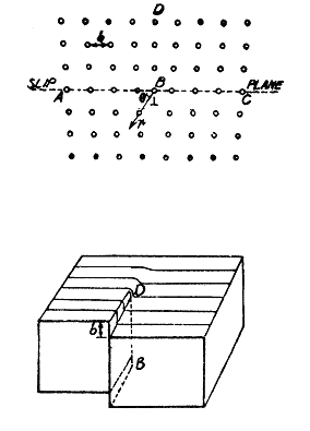
TYPE OF DISLOCATION The Edge Dislocation: Dislocation is a more complicated defect than any of the point defects. A dislocation is a region of a crystal in which the atoms are not arranged in the perfect crystal lattice. There are two extreme types of dislocations viz., the edge type and the screw type. Any particular dislocation is usually a mixture of these two types. An edge dislocation is the simplest one and a cross-sectional view of the atomic arrangement of atoms in it and the distortion of the crystal structure is shown in fig. 20. The part of the crystal above the slip plane at ABC has one more plane of atoms DB than the part below it. The line normal to the paper at B is called the dislocation line and the symbol ┴ at B is used to indicate the dislocation. The distortion is mostly present about the lower edge of the half plane of extra atoms and so the dislocation is that line of distortion which is near the end of the half plane. Hence a dislocation is a line imperfection as compared to the point imperfections considered before. In all the dislocations, the distortion is very intense near the dislocation line where the atoms do not have the correct number of neighbours. This region is called the core of dislocation. A few atom distances away from the centre, the distortion is very small and the crystal is almost perfect locally. At the core, the local strain is very high whereas it is so small at distances away form the core that the elasticity theory can be applied and it is called the elastic region. Another characteristic of the distortion of atomic arrangement in an edge dislocation is that the atoms just above the end of the extra half plane are in compression but just below the half plane the two rows of atoms to the right and left of the extra plane BD are farther apart from each other and the structure is expanded. This local expansion round an edge dislocation is called a dislocation. Besides the expansion and contraction near the dislocation, the structure is sheared also and this shear distortion is quite complicated.
Fig. 20 Fig. 21
Motion of a Dislocation: Dislocations can move just like the point defects move in the lattice but these are more constrained in motion because a dislocation must always be a continuous line. Motion of a dislocation is possible either by a climb or by a slip or by a glide. The motion of dislocation can give rise to a slip by a mechanism shown in fig. 22. When the upper half is pushed sideways by an amount b, then under the shear the motion of a dislocation tends to move the upper surface of the specimen to the right. Edge dislocations for which the extra half plane DB lies above the slip plane are called positive. If it is below the slip plane it is called negative edge dislocation. When an edge dislocation moves from one lattice site to another on the Fig. 22 slip plane, the atoms in the core move slowly so that the extra half plane at one lattice position becomes connected to a plane of atoms below the slip plane and the nearby plane of atoms becomes the new extra half plane. When finally the extra half plane BD reaches the right hand side of the block, the upper half of the block has completed the slip or glide by an amount b. Climb of a dislocation corresponds to its motion up or down from the slip plane. If the dislocation absorbs additional atoms from the crystal, it moves downward by substituting these atoms below B in the lattice. If the dislocation absorbs vacancies it moves up as the atoms are removed one by one from above B from the lattice sites.
Fig. 22 STRESS FIELD OF DISLOCATION The Burger's Vector: The Burger's vector b denotes actually the dislocation-displacement vector. A dislocation can be very well described by a closed loop surrounding the dislocation line. This loop, called the Burger's circuit is formed by proceeding through the undisturbed region surrounding a dislocation in steps which are integral multiples of a lattice translation. The loop is completed by going an equal number of translation in a positive sense and negative sense in a plane normal to the dislocation line. Such a loop must close upon itself if it does not enclose a dislocation, or fail to do so by an amount called a Burger's vector s = naa + nbb + ncc Where na, nb, nc are equal to integers or zero and a, b, c are the three primitive lattice translations.
Fig. 23
where b is the Burger's vector which measures the strength of the distortion caused by the dislocation, r is the radial distance from the point to the dislocation line and
where the z-axis lies along the dislocation and u, is the displacement in that direction. The angle
Let us have a cylindrical shell of a material surrounding an axial screw dislocation. Let the radius of the shell be r and the thickness dr, The circumference of the shell is
Fig. 24 and the corresponding shear stress in the good region is, where G is the shear modulus or modulus of rigidity of the material. A distribution of forces is exerted over the surface of the cut for producing a displacement b and the work done by the forces to do it gives the energy Es of the screw dislocation. Hence,
 (13) (13)
where F is the average force per unit area at a point on the surface during the displacement and the integral extends over the surface area of the cut. The average value is to be taken because the force at a point builds up linearly from zero to a maximum value as the displacement is produced. Thus the average force
is half the final value when the displacement is b i.e., Putting it in (13), we get
But dA = dz sr and so for a dislocation of length l, we have Thus, total elastic energy per unit length of a screw dislocation is given by where R and r0 the proper upper and lower limits of r. The energy depends upon the values taken for R and r0 is suitable when it is equal to about the Burger's vector b or equal to one or two lattice constants and the value of R is not more than the size of the crystal. Actually, however in most cases K is very much smaller than the size of the crystal. The value of R/r0 is not important as it occurs in the logarithmic term. Stress field of an edge dislocation: The calculation of the stress field is done on the assumption that the medium is isotropic having a shear modulus G and Poisson's ratio ʋ Let us consider the cross-section of a cylindrical material of radius R whose axis is along the z-axis and in which a cut has been in the plane y = 0, which becomes the slip plane. The portion above the cut is now slipped to the left by an amount b, the Burger's vector along the x-axis so that the new position assumes the shape shown dotted in fig. 25. Thus, a positive edge dislocation has been produced along the z-axis. Let σrr be the radial tensile stress, ie, compression or tension along the radius r and let σθθ be the circumferential tensile stress i.e., compression or tension acting in a plane perpendicular to r. Let τ rθ denote the shear stress acting in a radial direction. As seen from fig. 20, it is an odd function of x, considering the plane y = 0 and is found to be proportional to (cos
 are given by the following : . are given by the following : .
and
Fig. 25 does not hold as the stresses near a dislocation are very large. To know the value of ro, let us put ro = b, the magnitude of the strain there is then of the order of 1/2π(1-v)≈1/4 which is too much large to be treated by Hooke's law. We shall now calculate the energy of formation of an edge dislocation of unit length. The final shear stress in the plane y = 0 is given by (19) by putting θ = 0. For a cut along z-axis in a unit length, the strain energy for edge dislocation will be given by
 ….(20) ….(20)
This shows that the energy of formation becomes infinite if R becomes infinite. But even in large crystals the stress field are actually displaced some distance by other dislocation so that R = 10-3 cm. Assuming r0 = 5 ´10-8 cm. for a dislocation in copper Ee = 3´10-4 erg/cm = eV/atom plane Since G = 4 ´1011 dynes/cm2 b = 2.5´10-8 cm. and v = 0.34 In the case of screw dislocations its value is about (2/3) of this. The core energy of edge dislocation should be added to the elastic strain energy but it is of the order of 1eV per atom plane which is much less than the elastic strain energy and can be neglected. For a screw dislocation in the Z-direction in a cylindrical material, the stress field is given by a shear stress, according to (12).
Fig. 26 Low angle grain boundary (a) Two crystals Joined Together (b) Grain boundary formed with 2 rows of dislocations. There is no tensile and compress ional stress in this expression and this is perhaps due to the fact that there is no extra half plane in a screw dislocation. Also in this case the stresses are independent of θ expecting thereby that the stress field is cylindrically symmetric.
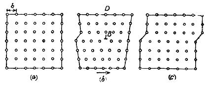
GRAIN BOUNDARIES Burger suggested that the boundaries of two crystallites or crystal grains at a low angle inclination with each other can be . Considered to be a regular array of dislocations. Two such crystallites placed close together at a small angle θ have been shown in fig. 26 (a). There are simple cubic crystals with
their axes perpendicular to the plane of the paper and parallel. The crystals have been rotated by θ /2 left and right of these axes. The results of joining the two crystals together is shown in fig. 26 (b). A grain boundary of the simple example of Burger's model is formed. The boundary plane contains a crystal axis common to the two crystals. Such a boundary is called a pure tilt boundary. Crystal orientations on both sides of the boundary plane are symmetric with each other such a boundary has a vertical arrangement of more than two edge dislocations of same sign. This arrangement is also stable as that for two dislocations. From the figure it is seen that the interval D between the dislocations so formed is given by Where b is the Burger’s vector of the dislocations and q is small Burger’s model of low angle grain boundary has been was confirmed experimentally by Vogel and co-workers for germanium single crystals. A germanium crystal was grown from a seeded melt along <100> direction. When the surface of this crystal was etched with a suitable chemical (acid), the terminus of a dislocation at the surface become a nucleus of the etching. action and a row of each pits was formed. It is shown diagrammatically in fig. 27. On examining these boundaries under very high optical magnification they were found to consist of regularly spaced conical pits. By counting the number of these etch pits, we are able to find out the number of dislocations in the crystal grain boundaries. The distance D between the pits is obtained by counting. The relative inclination angle q was also measured by means of X –ray diffraction experiments. From this value of q and knowing the value of b = 4.0 A0 in germanium, the value of D was calculated theoretically. This was found to be in very good agreement with the experimental etch pit interval.
Angle grain boundary in Ge If q is less than 50, the value of D is quite large as compared with the interatomic distance and so each dislocation can be considered as isolated. If q is about 150 than D is only a few interatomic distance and we get a collection of irregular, diffused and deformed vacancies. At present the etch pit method is the most direct method of determining the dislocation density. The density of dislocations is the number of dislocation lines which intersect a unit area in the crystal. It ranges from 102 – 103 in the best germanium and silicon crystals to 1011 – 10‑12 dislocations/cm2 in heavily deformed metal crystals. The density of dislocations can be estimated in solids by the following methods: (i) By plastic deformation of crystals, just like the bending of a pack of playing cards. (ii) By X-ray transmission method. (iii) By X-ray reflection. (iv) By electron microscopy (v)
(vi) By measurement on magnetic saturation of cold- worked fermagnetic materials. (vii) .By decoration methods. Decorated helical dislocations can be produced in calcium fluoride by decorating particles of CaO. (viii) By etch pit methods. 1.13 ETCHING- TYPES OF ETCHING In order to form a functional Micro-Electro-Mechanical Systems (MEMS) structure on a substrate, it is necessary to etch the thin films previously deposited and/or the substrate itself. In general, there are two classes of etching processes: 1.Wet etching where the material is dissolved when immersed in a chemical solution 2.Dry etching where the material is sputtered or dissolved using reactive ions or a vapor phase etchant In the following, we will briefly discuss the most popular technologies for wet and dry etching. Wet etching: This is the simplest etching technology. All it requires is a container with a liquid solution that will dissolve the material in question. Unfortunately, there are complications since usually a mask is desired to selectively etch the material. One must find a mask that will not dissolve or at least etches much slower than the material to be patterned. Secondly, some single crystal materials, such as silicon, exhibit anisotropic etching in certain chemicals. Anisotropic etching in contrast to isotropic etching means different etch rates in different directions in the material. The classic example of this is the <111> crystal plane sidewalls that appear when etching a hole in a <100> silicon wafer in a chemical such as potassium hydroxide (KOH). The result is a pyramid shaped hole instead of a hole with rounded sidewalls with a isotropic etchant. The principle of anisotropic and isotropic wet etching is illustrated in the figure below. This is a simple technology, which will give good results if you can find the combination of etchant and mask material to suit your application. Wet etching works very well for etching thin films on substrates, and can also be used to etch the substrate itself. The problem with substrate etching is that isotropic processes will cause undercutting of the mask layer by the same distance as the etch depth. Anisotropic processes allow the etching to stop on certain crystal planes in the substrate, but still results in a loss of space, since these planes cannot be vertical to the surface when etching holes or cavities. If this is a limitation for you, you should consider dry etching of the substrate instead. However, keep in mind that the cost per wafer will be 1-2 orders of magnitude higher to perform the dry etching
UNIT –I DEFECTS IN CRYSTALS Structure Introduction 1.1 Objectives 1.2 Point Defect in ionic crystals and metals 1.3 Diffusion in solids 1.3.1 Type of Diffusion 1.3.2 Diffusion Mechanisms 1.3.3 Diffusion Coefficient 1.3.4 Applications 1.4 Ionic Conductivity 1.5 Colour Centres 1.5.1 F- Centres 1.5.2 V-Centres 1.6 Excitions 1.7 General Idea of Luminescence 1.8 Dislocations & Mechanical Strength of Crystals 1.9 Plastic Bahaviour 1.10 Type of Dislocations 1.11 Stress field of Dislocations 1.12 Grain Boundaries 1.13 Etching- Types of Etching 1.14 Let Us Sum Up 1.15 Check Your Progress: The Key
INTRODUCTION
Up to now, we have described perfectly regular crystal structures, called ideal crystals and obtained by combining a basis with an infinite ·space lattice. In ideal crystals atoms were arranged in' a regular way. However, the structure of real crystals differs from that of ideal ones. Real crystals always have certain defects or imperfections, and therefore, the arrangement of atoms in the volume of a crystal is far from being perfectly regular. Natural crystals always contain defects, often in abundance, due to the uncontrolled conditions under which they were formed. The presence of defects which affect the colour can make these crystals valuable as gems, as in ruby (chromium replacing a small fraction of the aluminium in aluminium oxide: Al203). Crystal prepared in laboratory will also always contain defects, although considerable control may be exercised over their type, concentration, and distribution.
Key a = vacancy (Schottky defect) b = interstitial c = vacancy – interstitial pair (Frenkel defect) d = divacancy e = split interstitial
|
|||||||||||||||||||||||||||||||||||||||||||||||||||||||||||||||||||||||||||||||||||||||||||||||||||||||||||||||||||
Последнее изменение этой страницы: 2019-04-19; Просмотров: 254; Нарушение авторского права страницы
 There are some properties of materials such as stiffness, density and electrical conductivity which are termed structure-insensitive, are not affected by the presence of defects in crystals while there are many properties of greatest technical importance such as mechanical strength, ductility, crystal growth, magnetic

 (2)
(2)


 (4)
(4) (4a)
(4a)
 (5)
(5) (5a)
(5a)  (5a)
(5a) is a normalization factor. The diffusion coefficient D (m2/s) determines the rate of diffusion at a concentration gradient equal to unity. It depends on the composition of alloy, size of grains, and temperature.

 Now, we may discuss few applications in some detail. A common example of solid state diffusion is surface hardening of steel, commonly used for gears and shafts. Steel parts made in low carbon steel are brought in contact with hydrocarbon gas like methane (CH4) in a furnace atmosphere at about 9270C temperature. The carbon from CH4 diffuses into surface of steel part and theory carbon concentration increases on the surface. Due to this, the hardness of the surface increase. We may note that percentage of carbon diffuses in the surface increases with the exposure time. The concentration of carbon is higher near the surface and reduces with increasing depth Fig. (9)
 1.5.1 F Centres: The simplest and the most studied type of colour centre is an F centre. It is called an F centre because its name comes from the German word Farbe which means colour. F centres are generally produced by heating a crystal in an excess of an alkali vapour or by irradiating the crystal by X rays, NaCl is a very good example having F centres. The main absorption band in NaCl occurs at about


 (7)
(7) denotes the critical shear strees which we have to calculate For x << a, we have as usual,
 (8)
(8)
 is the elastic strain
 (9)
(9)
 (10)
(10)


 is the angle between the radius vector and the slip plane .as shown in fig. 20. Similarly, the atoms which are on a sheared lattice in a screw dislocation being on a spiral ramp, are displaced from their original positions in the perfect crystal according to the equation of a spiral ramp i.e.
 is measured from one axis perpendicular to the dislocation. Thus when
  increases by
  the displacement increases by a quantity b, the Burger's vector, which measures the strength of the dislocation. The Burger’s vector of a screw dislocation is parallel to the dislocation line while that of an edge dislocation, it is Perpendicular to the dislocation line and lies in the slip plane. In general cases, the Burger's vector may have other directions with respect to the dislocation and for these cases the dislocation is a mixture of both edge and screw types. Thus the mixed dislocation is defined in terms of the direction of the Burger's vector.
 and let it be sheared by an amount b, so that the shear strain
 (11)
(11)  (12)
(12)
 (14)
(14)

 (17)
(17) /r) because we require a function which varies as 1/r and which changes sign when y changes sign. Also it can be shown dimensionally that the constants of proportionality in the stress vary as G and b.
 ……(18)
 …..(19)
 where the positive values of σ are for tension and negative values for compression. Above the slip plane σrr is negative giving a compression, below the slip plane, it corresponds to a tensile stress. It may be noted that for r = 0, the stresses become infinite and so a small cylindrical region of radius ro around the dislocation must be excluded. This is necessary because in the bad region, the theory of elasticity
 …….(21)
 …….(22)
