|
Архитектура Аудит Военная наука Иностранные языки Медицина Металлургия Метрология Образование Политология Производство Психология Стандартизация Технологии |
|
|
Архитектура Аудит Военная наука Иностранные языки Медицина Металлургия Метрология Образование Политология Производство Психология Стандартизация Технологии |
GENERAL IDEA OF LUMINESCENCE
When a substance absorbs energy in some form or other, a fraction of the absorbed energy may be re-emitted in the form of electromagnetic radiation in the visible or near-visible region of the spectrum. This phenomenon is called luminescence, with the understanding that this term does not include the emission of blackbody radiation, which obeys the laws of Kirchhoff and Wien. Luminescent solids are usually referred to as phosphors. Luminescence is a process, which involves at least two steps: the excitation of the electronic system of the solid and the subsequent emission of photons. These steps may or may not be separated by intermediate processes. Excitation may be achieved by bombardment with photons (photoluminescence: with electrons (cathodo luminescence), or with other particles. Luminescence can also be induced as the result of a chemical reaction (chemi luminescence) or by the application of an electric field (electro luminescence)
One of the most important conclusions reached already in the early studies of luminescence, is that frequently the ability of a material to exhibit luminescence is associated with the presence of activators. These activators may be impurity atoms occurring in relatively small concentrations in the host material, or a small stoichiometric excess of one of the constituents of the material. In the latter case one speaks of self-activation. The presence of a certain type of impurity may also inhibit the luminescence of other centers, in which case the former are referred to as "killers." Since small amounts of impurities may play such an important role in determining the luminescent properties of solids, studies aimed at a better understanding of the mechanism of luminescence must be carried out with materials prepared under carefully controlled conditions. A great deal of progress has been made in this respect during the last two decades. A number of important groups of luminescent crystalline solids may be mentioned here.
(ii) The alkali halides activated with thallium or other heavy metals.
(iii) ZnS and CdS activated with Cu, Ag, Au, Mn, or with an excess of one of their constituents (self-activation).
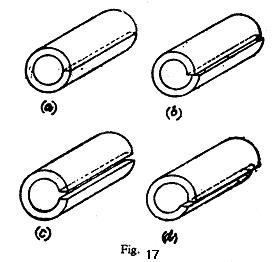
(iv) The silicate phosphors, such as zinc orthosilicate (willernite, Zn2Si04) activated with divalent maganese, which is used as oscilloscope screens. (v) Oxide phosphors, such as self-activated ZnO and Al203 activated with transition metals. (vi) Organic crystals, such as anthracene activated with naphtacene these materials are often used as scintillation counters. 1.8 DISLOCATIONS & MECHANICAL STRENGTH OF CRYSTALS The first idea of dislocations arose in the nineteenth century by observations that the plastic deformation of metals was caused by the formation of slip bands in which one portion of the material sheared with respect to the other. Later with the discovery that metals were crystalline it became more evident that such slip must represent the shearing of one portion of a crystal with respect to the other upon a rational crystal plane. Volterra and Love while studying the elastic behaviour of homogene-ous isotropic media considered the elastic properties of a cylinder cut in the forms shown in Figs. 17 (a) to (d), some of the deformation operations correspond to slip while some of the resulting configurations correspond to dislocation. The work on crystalline slip was then left out till dislocations were postulated as crystalline defects in the late 1930's. The configuration (a) shows the cylinder as originally cut (b) and (c) correspond to edge dislocations while (d) corresponds to screw dislocation.
After the discovery of X-rays, Darwin and Ewald found that the intensity of X-ray beams reflected from actual crystals was about 20 times greater than that expected from a perfect crystal. In a perfect crystal, the intensity is low due to long absorption path given by multiple internal reflections. Also, the width of the reflected beam from an actual crystal is about 1 to 30 minutes of an are as compared with that expected for a perfect crystal which is only about a few seconds. This discrepancy was explained by saying that the actual crystal consisted of small, roughly equiaxed crystallites, 10-4 to 10-5 cm. In diameter, slightly misoriented with respect to one another, with the boundaries between them consisting of amorphous material. This is the "mosaic block" theory in which the size of the crystallites limits the absorption path and increases the intensity. The misorientation explains the width of the beam. It was however found recently that the boundaries of the crystallites are actually arrays of dislocation lines. The presence of dislocation lines is also proved by the study of crystal growth. Volmer's and Gibbe's theoretical study on nucleation of new layers showed that the layer growth of perfect crystals is not appreciable until supersaturation of about 1.5 were attained. However, experimental work of Volmer and Schultze on iodine showed that crystals grew under nearly equilibrium conditions. Frank removed this discrepancy by saying that the growth of crystals could take place at low supersaturations by the propagation of shelves associated with the production of a dislocation at the surface.
Mechanical Strength of Crystal : The weakness of good crystals was a mystery for many years, in part, no doubt, because the observed data easily led one to the wrong conclusion. Relatively poorly prepared crystal were found to have yield strengths close to the high value we first estimate for the perfect crystal. However, as the crystals were improved (for example, by annealing) the yield strengths were found to drop drastically, falling by several orders of magnitude in very well prepared crystals. It was natural to assume that the yield strength was approaching that of a perfect crystal as specimens were improved, but, in fact, quite the opposite was happening. Three people independently came up with the explanation in 1943, inventing the dislocation to account for the data. They suggested that almost all real crystals contain dislocations, and that plastic slip occurs through their motion as described above. There are then two ways of making a strong crystal. one is to make an essentially perfect crystal, free of all dislocation. This is extremely difficult to achieve. Another way is to arrange to impede the flow of dislocations, for although dislocations move with relative ease in a perfect crystal, if they work required to move them can increase considerably. Thus the poorly prepared crystal is hard because it is infested with dislocations and defects, and these interfere so seriously with each other's motion that slip can occur only by the more drastic means described earlier. However, as the crystal is purified and improved, dislocation largely move out of the crystal, vacancies and interstitials are reduced to their (low) thermal equilibrium concentrations, and the unimpeded motion of those dislocations that remain makes it possible for the crystal to deform with c\ease. At this point the crystal is very soft. If one could continue the process of refinement to the point where all dislocations were removed, the crystal would again become hard.
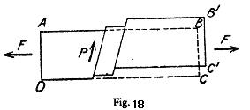
Plastic deformation takes place in a crystal due to the sliding of one part of a crystal with respect to the other. This results in slight increase in the length of the crystal ABCD under the effect of a tension FF applied to it as shown in fig. 18. The 'process of sliding is called slip. The direction and place in which the sliding takes place are called respectively the slip direction as shown by the arrow P and slip plane. The outer surface of the single crystal is deformed and a slip band is formed, as is seen in the figure, which may be several thousand Angstroms wide. This can be observed by means of an optical microscope, but when observed by an electron microscope a slip band is found to consist of several slip lamellae. The examination of slips by an electron microscope reveals that these extend over several tens of lattice constants. The slip lines do not run throughout the crystal but end inside it, showing that slips do not take place simultaneously over the whole Slip planes but occur only locally. The study of slips in detail tells us that plastic deformation is inhomogeneous i.e., only a small number of those atoms take part in the slip which form layers on either side of a slip plane. In the case of elastic deformation all atoms in the crystal are affected and its properties can be understood in terms of interatomic forces acting in a perfect lattice. On the other hand, plastic deformation cannot be studied by simply extending elasticity to large stresses and strains or on the basis of a perfect lattice. We will now prove below that for plastic flow in a perfectly periodic lattice, we have to apply very much larger stresses (~ 1010 dynes per cm2) than those required for the normal plastic flow observed in actual crystals (~106
Shear Strength Crystals: J. Frenkel in calculating the theoretical shear strength of a perfect crystal. The model proposed by him is given in fig. 19, showing a cross-section through two adjacent atomic planes separated by a distance d. The full line circles indicate the equilibrium positions of the atoms without any external force.
Fig. 19
shear stress t has been plotted as a function of the relative displacement of the planes from their equilibrium positions and this gives the periodic behavior of t as supposed by Frenkel. ' t is found to become zero for x = 0, a/2, a etc., where a is the distance between the atoms in the direction of the shear. Frenkel assumed that this periodic function is given by where the amplitude In order to calculate the force required to shear the two planes of atoms, we from the definition of shear modulus
where G is the shear module and
or This gives the maximum critical stress above which the crystal becomes unstable. It is about one sixth of the shear modulus. In a cubic crystal, G c44 = 1011 dynes per cm. for a shear in the <100> direction. Hence the theoretical value of the critical shear stress on Frenkel's model is tc = 1010 dynes per sq. .cm. which is much larger than the observed values for pure crystals. However., the experimental values for the maximum resolved shear stress required to start the plastic flow in metals were of the order of 10-3 to 10-4 G at that time and it was not a agreement with the results of eqn.. (10) Later it was considered that eqn (10) gave a higher value as the different semi-inter –atomic force of Fig.19 (b) as taken by Frenkel. The above disagreement may also be due to other special configuration of mechanical stability which the lattice may develop when it is sheared. Mackenzie in 1949, using central forces in the case of close packed lattices found that tc could be reduced to a value G/30 , corresponding to a critical shear strain of about 20 This value, however, is supposed to be an underestimate due to the neglect of the small directional force which are also present in such lattices. The contributions of thermal stresses also reduce tc below G/30 only near the melting point. Thus at room temperature we should have G/5 > tc > G/30 i.e. = G/15. In the case of whiskers only,. the experimental value of tc for various metals has been found to be of this order which is in excellent agreement with the theoretical result. Recent experimental work on bulk copper and zinc has shown that plastic deformation being at stresses of the order of 10-9 G. Hence, except for whiskers the disagreement is even larger than before.. It is therefore clear that agreement between theory and experiment be obtained on the basis of Frenkel's model where atomic plant glide past each other assuming fig. 19 (a) that the atoms of the upper atomic plane move simulantaneously relative to the lower plane. This assumption is based on the supposition of a perfect lattices, and that is the main cause of difficulty. We have , therefore, to consider the presence of imperfections which act as sources of mechanical weakness in actual crystals and which may proud a slip by the consecutive motion of the atoms but not by simultaneous motion of the atoms of one plane relative to another. After Frenkel theory Masing and Polanyi, Pradtl and Dehlinger proposed different defects but in 1934, Orowan, Polanyi, and Taylor proposed edge dislocation, while in
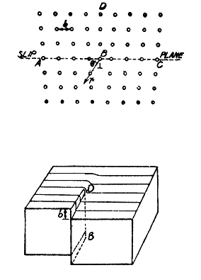
TYPE OF DISLOCATION The Edge Dislocation: Dislocation is a more complicated defect than any of the point defects. A dislocation is a region of a crystal in which the atoms are not arranged in the perfect crystal lattice. There are two extreme types of dislocations viz., the edge type and the screw type. Any particular dislocation is usually a mixture of these two types. An edge dislocation is the simplest one and a cross-sectional view of the atomic arrangement of atoms in it and the distortion of the crystal structure is shown in fig. 20. The part of the crystal above the slip plane at ABC has one more plane of atoms DB than the part below it. The line normal to the paper at B is called the dislocation line and the symbol ┴ at B is used to indicate the dislocation. The distortion is mostly present about the lower edge of the half plane of extra atoms and so the dislocation is that line of distortion which is near the end of the half plane. Hence a dislocation is a line imperfection as compared to the point imperfections considered before. In all the dislocations, the distortion is very intense near the dislocation line where the atoms do not have the correct number of neighbours. This region is called the core of dislocation. A few atom distances away from the centre, the distortion is very small and the crystal is almost perfect locally. At the core, the local strain is very high whereas it is so small at distances away form the core that the elasticity theory can be applied and it is called the elastic region. Another characteristic of the distortion of atomic arrangement in an edge dislocation is that the atoms just above the end of the extra half plane are in compression but just below the half plane the two rows of atoms to the right and left of the extra plane BD are farther apart from each other and the structure is expanded. This local expansion round an edge dislocation is called a dislocation. Besides the expansion and contraction near the dislocation, the structure is sheared also and this shear distortion is quite complicated.
Fig. 20 Fig. 21
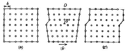
Motion of a Dislocation: Dislocations can move just like the point defects move in the lattice but these are more constrained in motion because a dislocation must always be a continuous line. Motion of a dislocation is possible either by a climb or by a slip or by a glide. The motion of dislocation can give rise to a slip by a mechanism shown in fig. 22. When the upper half is pushed sideways by an amount b, then under the shear the motion of a dislocation tends to move the upper surface of the specimen to the right. Edge dislocations for which the extra half plane DB lies above the slip plane are called positive. If it is below the slip plane it is called negative edge dislocation. When an edge dislocation moves from one lattice site to another on the Fig. 22 slip plane, the atoms in the core move slowly so that the extra half plane at one lattice position becomes connected to a plane of atoms below the slip plane and the nearby plane of atoms becomes the new extra half plane. When finally the extra half plane BD reaches the right hand side of the block, the upper half of the block has completed the slip or glide by an amount b. Climb of a dislocation corresponds to its motion up or down from the slip plane. If the dislocation absorbs additional atoms from the crystal, it moves downward by substituting these atoms below B in the lattice. If the dislocation absorbs vacancies it moves up as the atoms are removed one by one from above B from the lattice sites.
Fig. 22 |
Последнее изменение этой страницы: 2019-04-19; Просмотров: 233; Нарушение авторского права страницы
 dynes per cm2).
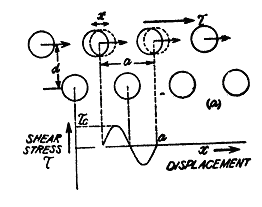
 (7)
(7) denotes the critical shear strees which we have to calculate For x << a, we have as usual,
 (8)
(8)
 is the elastic strain
 (9)
(9)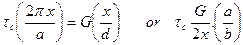
 (10)
(10)