|
Архитектура Аудит Военная наука Иностранные языки Медицина Металлургия Метрология Образование Политология Производство Психология Стандартизация Технологии |
|
|
Архитектура Аудит Военная наука Иностранные языки Медицина Металлургия Метрология Образование Политология Производство Психология Стандартизация Технологии |
Fig. 7. Time dependence of diffusion (Fick’s second law)
Dependence of Diffusion Coefficient on Temperature The diffusion coefficient D (m2/s) determines the rate of diffusion at a oncentration gradient equal unity. It depends on the composition of alloy, size of grains, and temperature. The dependence of diffusion coefficient on temperature in a certain temperature range is described by Arrhenius exponential relationship D = D0 exp (-Q/RT) (6)
Factors Affecting Diffusion Coefficient (D) We have mentioned that diffusion co-efficient is affected by concentration. However, this effect is small compared to the effect of temperature. While discussion diffusion mechanism, we have assumed that atom jumped from one lattice position to another. The rate at which atoms jumped mainly depends on their vibrational frequency, the crystal structure. Activation energy and temperature we may note that at the position. To overcome this energy barrier, The energy required by the atom is called the activation of diffusion (Fig. 8)
Fig. 8. Activation energy for diffusion (a) vacancy mechanism (b) interstitial mechanism The energy is required to pull the atom away from its nearest atoms in the vacancy mechanism energy is also required top force the atom into closer contact with neighbouring atoms as it moves along them in interstitial diffusion. If the normal inter- atomic distance is either increases or decrease, addition energy is required. We may note that the activation energy depends on the size of the atom. i.e. it varies with the size of the atom, strength of bond and the type of the diffusion mechanism. It is reported that the activation energy required is high for large- sized atoms, strongly bonded material , e.g. corundum and tungsten carbide (since interstitial diffusion requires more energy than the vacancy mechanism.)
Diffusion processes are the basis of crystallization recrystallization, phase transformation and saturation of the surface of alloys by other elements, Few important applications of diffusion are : (i) Oxidation of metals (ii) Doping of semiconductors. (iii) Joining of materials by diffusion bonding, e.g. welding, soldering, galvanizing, brazing and metal cladding (iv) Production of strong bodies by sintering i.e. powder metallurgy. (v) Surface treatment , e.g. homogenizing treatment of castings , recovery, recrystallization and precipitation of phases. (vi) Diffusion is fundamental to phase changed e.g. y to a-iron.
Fig. 9. C gradient in 1022 steel carburized in 1.6% CH4, 20% CO and 4%H.
Check Your Progress 3 Notes : (i) Write your answer in the space given below (ii) Compare your answer with those given at the end of the unit What is diffusion and on what variable it depends? ……………………………………………………………………………………… ……………………………………………………………………………………… ……………………………………………………………………………………… ………...……………………………………………………………………………
IONIC CONDUCTIVITY
It is known that the dominant lattice defect responsible for the ionic conductivity in pure and doped lead chloride is the anion vacancy (Jost 1952). The activation energy for migration of the anion vacancy has been measured by Simkovich (1963), Seith (De Vries 1965) and Gylai (De Vries 1965) in powder samples and is found to range from 0-48 eV to 0-24 eV. The measurements on single crystals of pure and doped lead chloride, however, show that the energy of formation of vacancies is 1-66 eV and that for migration of the anion vacancies is 0-35 eV (De Vries and Van Santen 1963; De Vries 1965). Theroles of various point defects in this material are not yet clearly understood. Simkovich, fox example, concluded that in the extrinsic region half of the anion vacancies are associated with cation vacancies to form charged pairs. Barsis and Taylor (1966), on the other hand, proposed that appreciable number of inteistitials, i.e., unassociated Frenkel defects, are present in the extrinsic region as seen from the analysis of isotherms obtained by them from the data of De Vries and Van Santen. The recent experiments by Van den Brom etal (1972) on the dielectric relaxation in pure lead chloride suggest that in this region dipole species such as anion vacancy-impurity associates are piesent. In this paper, we shall present the results of self-diffusion and ionic conductivity measurements made on pure crystals of lead chloride, and show that ir this material Schottky defects are mainly responsible for the observed ionic transport and that the impurity anion vacancy associates, particularly the oxygen ions, influence it markedly in the extrinsic region.
1.5 COLOUR CENTRES Colour centres: Becquerel discovered that a transparent NaCl crystal was coloured yellowish when it was placed near a discharge tube. The colouration of the NaCl and other crystals was responsible for the study of colour centres. Actually, rocksalt should have an infrared absorption due to vibrations of its ions and an ultraviolet absorption due to the excitation of the electrons. A perfect NaCl crystal should not absorb visible light and so it should be perfectly transparent. This leads us to the conclusion that the colouration of crystals is due to defects in the crystals. It is also found that exposure of a coloured crystal to white light can result in bleaching of the colour. This gives further clues to the nature of absorption by crystals. Experiments show that during the bleaching of the crystal the crystal becomes photoconductive. i.e., electrons are excited to the conduction band. Photoconductivity tells us about the quantum efficiency (number of free electrons produced per incident photon) of the colour centres. It is known that insulators have large energy gaps and that they are transparent to visible light. Ionic crystals have the forbidden energy gap of about 6eV which corresponds to a wavelength of about 2000A0 in the ultraviolet region. From dielectric properties we know that the ionic polarizability resonates at a wavelength of 60 microns in the far infrared region. It is why these crystals are expected to be transparent over a wide range of spectrum including the visible region. Due to such a good transparency, the crystals of KCl, NaCl, LiF and other alkali halides are used for making prisms, lenses and optical windows in optical and infrared spectrometers. However, due to different reasons, absorption bands may occur in the visible, near ultraviolet and near infrared regions in these crystals. If the absorption band is in the visible region and the band is quite narrow, it gives a characteristic colour to the crystal. When the crystal gets coloured, it is said to have colour centres. Thus a colour centre is a lattice defect, which absorbs light.
(i) Crystals can be coloured by the addition of suitable chemical impurities like transition element ions with excited energy levels. Hence alkali halide crystals can be coloured by ions whose salts are normally coloured. (ii) The crystals can be coloured by introducing stoichiometric excess of the cation by heating the crystal in the alkali metal vapour and then cooling it quickly. The colours produced depend upon the nature of the crystals e.g., LiF heated in Li vapour colours it pink, excess of K in KCl colours it blue and an excess of Na in NaCl makes the crystal yellow. Crystals coloured by this method on chemical analysis show an excess of alkali metal atoms, typically 1016 to 1019 per unit volume. (iii) Crystals can also be coloured or made darker by exposing them to high energy radiations like X-rays or ϒ-rays or by bombarding them with energetic electrons or neutrons.
4650A 0 and it is called the F band. This absorption in the blue region is said to be responsible for the yellow colour produced in the crystal. The F band is characteristic of the crystal and not of the alkali metal used in the vapour i.e., the F band in KCI or NaCl will be the same whether the crystal is heated in a vapour of sodium or of potassium. The F bands associated with the F centres of some alkali halide crystals are shown in fig. 10, in which the optical absorption has been plotted against wavelength or energy in eV
Formation of F-Centres: Colour centres in crystals can be fanned by their non-stoichiometric properties i.e., when crystals have an excess of one of its constituents. NaCl crystal can therefore be coloured by heating it in an atmosphere of sodium vapour and then cooling it quickly. The excess sodium atoms absorbed from the vapour
Split up into electrons and positive ions in the crystal (fig. 11). The crystal becomes slightly non-stoichiometric, with more sodium ions than chlorine ions. This results in effect in CI- vacancies. The valence electron of the alkali atom is not bound to the atom, it diffuses into the crystal and becomes bound to a vacant negative ion site at F because a negative ion vacancy in a perfect periodic lattice has the effect of an isolated positive charge. It just traps an electron in order to maintain local charge neutrality. The excess electron captured in this way at a negative ion vacancy in an alkali halide crystal is called an F centre. This electron is shared largely by the six positive metal ions adjacent to the vacant negative lattice site as shown in 2-dimensions by the dotted circle in fig. 11. The figure shows an anion vacancy and an anion vacancy with an associated electron, i.e., the centre. This model was first suggested by De-Boer and was further developed by Mott and Gurney. Change of Density: Since some Cl- vacancies are always present in a NaCl crystal in thermodynamic equilibrium, any sort of radiation which will cause electrons to be knocked into the Cl- vacancies will cause the formation of F centres. This explains Becquerel's early results also. With that the generation of vacancies by the introduction of excess metal can be experimentally demonstrated by noting a decrease in the density of the crystal. The change of density is determined by X-ray diffraction measurements.
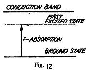
shows the energy level diagram for an F centre. It also shows that the F absorption band is produced due to a transition from the ground state to the first excited state below the conduction band. Effect of temperature on F-band: We have seen above that the energy levels of an F-centre depend upon the atomic surroundings of vacancy. This means that the absorption peak should shift to shorter wavelengths i.e., higher energies when the interatomic distances in the crystal are decreased. This shift is actually observed on varying the temperature of the crystal. The absorption maximum has a finite breadth even at very low temperature, which increases on increasing the temperature of the crystal. It can be explained by studying the dependence of the energy of-a colour centre on temperature. Fig. 13. Shows a graph plotted between the changes in energy of an electron in F centre and the coordination of a vacancy
state of that electron.
At any finite temperature the ground state is not at 0, the minimum of curve G but lies above it by about kE because the coordinating ions vibrate between A and B due to thermal energy. Hence the energy of the absorbed radiation can range between that of transition A → A` or B → B`. The difference between energies, corresponding to A` and B` gives the width of the absorption peak. AB represents the amplitude of vibration of ions at a lower temperature but as the temperature rises it moves to a higher energy position so that CD represents the amplitude of vibration at the higher temperature and thus the width of the absorption peak- the F band increases. Klcinschord observed that the F band instead of being exactly like a bell, ossesses a shoulder and a tail on the short wavelength side. Seitz called the shoulder as a K-band and it may be considered to be due to transitions of the electron to excited states, which lie between the first excited state and the conduction band. The tail may be supposed to be due to the transition from the ground state of F-centre to the conduction band. Magnetic Properties of F-Centres: In fig. 13, the upper curve E is determined by the change in the surroundings of a vacancy when the trapped electrons is in the excited state. This is usually expressed by a change of the effective dielectric constant in the neighbourhood of such a vacancy. An alkali halide crystal is normally diamagnetic because the ions have closed outer shells. Since an F-centre contains an unpaired trapped electron, crystals additively coloured with a metal have some paramagnetic behavior. Thus the structure of F-centres can be studied by electron paramagnetic resonance experiments which tell us about the wave-functions of the trapped electron.
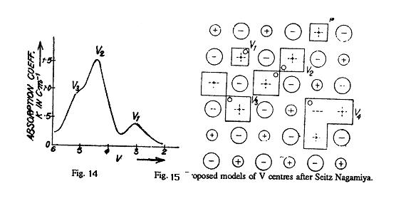
maxima which are called as V1, V2 bands and so on. Mollwo was able to introduce access halogen into KBr and KI and found that it is was not possible in case of KCl. He shows that by heating KI in iodine vapour ,new absorption bands are obtain in the ultraviolet .the bands obtain by Mollwo for KBr when heated in Br2 vapour are shown in fig. 14, having V1, V 2 and V3 bands.
It can be understood that the strong peak observed by Mollwo in KBr as shown in fig. 14 is however, not of the above type. Mollwo's experiment proves that the saturation density of colour centres is proportional to the number of bromine molecules at a particular temperature. By the law of mass action, we know that one colour centre should be produced by each molecule absorbed from the vapour. Hence it was proposed by F. Seitz that the centres associated with the strong peak are of molecular nature, i.e., two holes are trapped by two positive ion vacancies. Such a centre is called a V2 centre and is shown in fig. 15. As is evident from the figures 13 and 15, the V1 centre is the counterpart of the F-centre, V2 and V3 are those of the R centres and V 4 is the counterpart of the M centre. However, the identification of the V1 centre with the V 1 band is uncertain because the spin resonance results of Kaenzig suggest that a centre having the symmetry of the V3 centre produces the V1 band. The detailed properties of V centres have not yet been properly understood. Production or Colour Centres by X-rays or Particle Irradiation: The colour centres can also be produced in crystals by irradiating them with very high energy radiation like X -rays or ϒ rays. An X-ray quantum when passes through an ionic crystal produces fast photo electrons having the energy nearly equal to that of the incident quantum. These high energy electrons interact with the valence electrons in the crystal and lose their energy by producing free electrons and holes, excitons (electron hole pairs) and phonons. These free electrons and holes diffuse into the crystal and come across vacancies present in the crystal where they may be caught producing trapped electrons and holes. In this way both F and V types of colour centres are produced in crystals irradiated with high energy radiations. However, these are not permanent like those produced in non stoichiometric crystals in which there is an internally produced excess of electrons and holes. Their colours cannot be removed permanently without changing them chemically. The colour centres produced by X-ray radiation are easily bleached by visible light or by heating because the excited electrons and holes ultimately recombine with each

other. The F and V centres produced by irradiation with 30 keV X -rays at room temperature (20°C) have been shown in fig. 16 in the absorption spectrum of KCl taken by Dorendorf and Pick. Check Your Progress 4 Notes : (i) Write your answer in the space given below (ii) Compare your answer with those given at the end of the unit What are color centers and how do they affect electric conductivity of solids? ……………………………………………………………………………………… ……………………………………………………………………………………… ……………………………………………………………………………………… ………...……………………………………………………………………………
EXCITIONS The most obvious point defects consist of missing ions (vacancies), excess ions (interstitials), or the wrong kind of ions (substitution impurities). A more subtle possibilitials is the case of an ion in a perfect crystal, that differs from its colleagues only by being in an excited electronic state. Such a “defect” is called a Frenkel exciton. Since any ion is capable of being so excited, and since the coupling between the ions’ outer electronic shells is strong, the excitation energy can actually be transferred from ion to ion . Thus the Frenkel exciton can move through the crystal wit\hout the ions themselves having to change places, as a result of which it is (like the polaron) for more mobile than vacancies, interstitials, or substitutional impurities. Indeed, for more accurate to describe the electronics structure of a crystal containing an exciton, as a quantum mechanical superposition of states, in which it is equally probable that the excitation is associated with any ion in the crystal. This latter view bears the same relation to specific excited ions, as the Bloch tight – binding levels (Chapter 10) bear to the individual atomic levels, in the theory of band structures.
Suppose we have calculated the electronic ground state of an insulator in the independent electron approximation. The lowest excited state of the insulator willevidently be given by removing one electron from the highest level in the highest occupied band 9the valence band) and placing it into the lowest – lying level of the lowest unoccupied band (conduction band). Such a rearrangement of the distribution of electrons does not alter the self- consistent periodic potential in which they move. This is because the Bloch electron are not localized (since | ynk(r)|2 is periodic), and therefore the change in local charge density produced by changing the level of a single electron will be of order 1/N (since only an Nth of the electron's charge will be in any given cell) i.e. negligibly small. Thus the electronic energy levels do not have to be recomputed for the excited configuration and the first excited state will lie an energy ec -ev above the energy of the ground state, where ec is the conduction band minimum and ev the valence band maximum. However, there is another way to make an excited state. Suppose we form a one-electron level by superposing enough level near the conduction band minimum to form a well- localized wave packet. Because we need levels in the neighborhood of the minimum to produce the wave packet, the energy ec of the wave packet will be somewhat grater than ec. Suppose in addition that the valence band level we depopulate is also wave packet. , formed of levels in the neighborhood of the valence band maximum (so that its energy ev is somewhat less than ev) and chosen so that the center of the wave packet is spatially very near the center of the conduction band wave packet. If we ignored electron – electron interactions, the energy required to move an electron from valence to conduction band wave packet. If we ignored electron- electron interactions, the energy required to move an electron from valence to conduction band wave packets would be ec - ev > ec - ev, but because the levels are localized, there will, in addition, be a non – negligible amount of negative Coulomb energy due to the electrostatic attraction of the (localized) conduction band electron and (localized) valence band hole.
Let us consider the case in which the localized electron and hole levels extend over many lattice constants. We may then make the same type of semi classical argument that we used to deduce the form of the impurity levels in semiconductors. We regard the electron and hole as particles of mass mc and mv (the conduction and valence band effective masses, which we take, for simplicity, to be isotropic). They interact through an attractive Coulomb interaction screened by the dielectric constant Î of the crystal. Evidently this is just the hydrogen atom problem, with the hydrogen atom reduced mass m (1/m = 1/Mproton + 1/melectron » 1/melectron) replaced by the reduced effective mass m* (1/m* = 1/mc + 1/mv ) , and the electronic charge replaced by e2/Î. Thus there will be bound states, the lowest of which extends over a Bohr radius given by:.

the energy of the bound state will be lower than the energy (ec - ev ) of the non-interacting electron and hole by
The validity of this model requires that aex be large on the scale of the lattic (i.e., aex >>a0), but since insulators with small energy gaps tend to have small effective masses and large dielectric constants, that is no difficult to achieve, particularly in semiconductors. such hydrogenic spectra have in fact been observed in the optical absorption that occurs below the inter and threshold. The exciton described by this model is known as the Mott- Wannier exciton Evidently as the atomic levels out of which the band levels are formed become more tightly bound Îwill decrease m* will increases, a0* will decrease, the exciton will become more localized, and the Mott- Wannier picture will eventually break down. The Mott- Wannier exciton and the Frenkel exciton are opposite extremes of the same phenomenon. In the Frenkel case, based as it is on a single excited ionic level, the elelctron and hole are sharply localized on the atomic scale. The exciton spectra of the solid range gases fall in this class. |
Последнее изменение этой страницы: 2019-04-19; Просмотров: 300; Нарушение авторского права страницы

 Now, we may discuss few applications in some detail. A common example of solid state diffusion is surface hardening of steel, commonly used for gears and shafts. Steel parts made in low carbon steel are brought in contact with hydrocarbon gas like methane (CH4) in a furnace atmosphere at about 9270C temperature. The carbon from CH4 diffuses into surface of steel part and theory carbon concentration increases on the surface. Due to this, the hardness of the surface increase. We may note that percentage of carbon diffuses in the surface increases with the exposure time. The concentration of carbon is higher near the surface and reduces with increasing depth Fig. (9)
 1.5.1 F Centres: The simplest and the most studied type of colour centre is an F centre. It is called an F centre because its name comes from the German word Farbe which means colour. F centres are generally produced by heating a crystal in an excess of an alkali vapour or by irradiating the crystal by X rays, NaCl is a very good example having F centres. The main absorption band in NaCl occurs at about