|
Архитектура Аудит Военная наука Иностранные языки Медицина Металлургия Метрология Образование Политология Производство Психология Стандартизация Технологии |
|
|
Архитектура Аудит Военная наука Иностранные языки Медицина Металлургия Метрология Образование Политология Производство Психология Стандартизация Технологии |
Figure 28: Difference between anisotropic and isotropic wet etching.
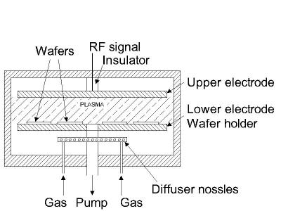
Dry etching: The dry etching technology can split in three separate classes called reactive ion etching (RIE), sputter etching, and vapor phase etching. In RIE, the substrate is placed inside a reactor in which several gases are introduced. A plasma is struck in the gas mixture using an RF power source, breaking the gas molecules into ions. The ions are accelerated towards, and reacts at, the surface of the material being etched, forming another gaseous material. This is known as the chemical part of reactive ion etching. There is also a physical part which is similar in nature to the sputtering deposition process. If the ions have high enough energy, they can knock atoms out of the material to be etched without a chemical reaction. It is a very complex task to develop dry etch processes that balance chemical and physical etching, since there are many parameters to adjust. By changing the balance it is possible to influence the anisotropy of the etching, since the chemical part is isotropic and the physical part highly anisotropic the combination can form sidewalls that have shapes from rounded to vertical. A schematic of a typical reactive ion etching system is shown in the figure below.
Sputter etching is essentially RIE without reactive ions. The systems used are very similar in principle to sputtering deposition systems. The big difference is that substrate is now subjected to the ion bombardment instead of the material target used in sputter deposition. Vapor phase etching is another dry etching method, which can be done with simpler equipment than what RIE requires. In this process the wafer to be etched is placed inside a chamber, in which one or more gases are introduced. The material to be etched is dissolved at the surface in a chemical reaction with the gas molecules. The two most common vapor phase etching technologies are silicon dioxide etching using hydrogen fluoride (HF) and silicon etching using xenon diflouride (XeF2), both of which are isotropic in nature. Usually, care must be taken in the design of a vapor phase process to not have bi-products form in the chemical reaction that condense on the surface and interfere with the etching process.
Figure 29: Typical parallel-plate reactive ion etching system.
Like anything else in this world, crystals inherently possess imperfections, or what we often refer to as 'crystalline defects'. The presence of most of these crystalline defects is undesirable in silicon wafers, although certain types of 'defects' are essential in semiconductor manufacturing. Engineers in the semiconductor industry must be aware of, if not knowledgeable on, the various types of silicon crystal defects, since these defects can affect various aspects of semiconductor manufacturing - from production yields to product reliability. Crystalline defects may be classified into four categories according to their geometry. These categories are: 1) zero-dimensional or 'point' defects; 2) one-dimensional or 'line' defects; 3) two-dimensional or 'area' defects; and 4) three-dimensional or 'volume' defects. Table 2 presents the commonly-encountered defects under each of these categories.
Table 2. Examples of Crystalline Defects
There are many forms of crystal point defects. A defect wherein a silicon atom is missing from one of these sites is known as a 'vacancy' defect. If an atom is located in a non-lattice site within the crystal, then it is said to be an 'interstitial' defect. If the interstitial defect involves a silicon atom at an interstitial site within a silicon crystal, then it is referred to as a 'self-interstitial' defect. Vacancies and self-interstitial defects are classified as intrinsic point defects.
If an atom leaves its site in the lattice (thereby creating a vacancy) and then moves to the surface of the crystal, then it becomes a 'Schottky' defect. On the other hand, an atom that vacates its position in the lattice and transfers to an interstitial position in the crystal is known as a 'Frenkel' defect. The formation of a Frenkel defect therefore produces two defects within the lattice - a vacancy and the interstitial defect, while the formation of a Schottky defect leaves only one defect within the lattice, i.e., a vacancy. Aside from the formation of Schottky and Frenkel defects, there's a third mechanism by which an intrinsic point defect may be formed, i.e., the movement of a surface atom into an interstitial site.
Extrinsic point defects, which are point defects involving foreign atoms, are even more critical than intrinsic point defects. When a non-silicon atom moves into a lattice site normally occupied by a silicon atom, then it becomes a 'substitutional impurity.' If a non-silicon atom occupies a non-lattice site, then it is referred to as an 'interstitial impurity.' Foreign atoms involved in the formation of extrinsic defects usually come from dopants, oxygen, carbon, and metals. The presence of point defects is important in the kinetics of diffusion and oxidation. The rate at which diffusion of dopants occurs is dependent on the concentration of vacancies. This is also true for oxidation of silicon. Crystal line defects are also known as 'dislocations', which can be classified as one of the following: 1) edge dislocation; 2) screw dislocation; or 3) mixed dislocation, which contains both edge and screw dislocation components. An edge dislocation may be described as an extra plane of atoms squeezed into a part of the crystal lattice, resulting in that part of the lattice containing extra atoms and the rest of the lattice containing the correct number of atoms. The part with extra atoms would therefore be under compressive stresses, while the part with the correct number of atoms would be under tensile stresses. The dislocation line of an edge dislocation is the line connecting all the atoms at the end of the extra plane.

|
Последнее изменение этой страницы: 2019-04-19; Просмотров: 310; Нарушение авторского права страницы